|
|
|
|
|
|

The use of SimuLase™ for the typical example of an edge-emitter and a VECSEL
are described in the examples guide.
• InGaAsP-based edge-emitter operating at 1.3µm, carrier losses and resulting threshold currents in an:
• InGaSb/InAs/AlGaSb type-II 'W' structure operating at 3.4µm, and some more examples for
• Gain in an InGaN/GaN multi quantum well, More examples can be found in the listed publications.
A detailed explanation on how to use SimuLase™
for the examples of an edge emitting ridge waveguide structure and a VECSEL structure,
including theory-experiment comparisons for all important aspects,
ranging from the PL to the input-output characteristics,
can be found here.
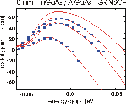
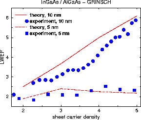
Screen grabs from SimuLase in the analysis of an edge-emitting structure (top) and a VECSEL (bottom). InGaSb/InAs/AlGaSb 'W' structure for 3.4µm 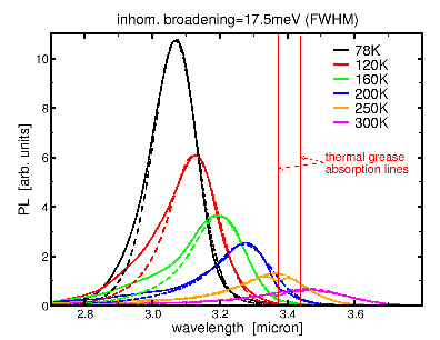 Experimentally measured (solid lines) and calculated (dashed lines) temperature dependent PL spectra for a mid-infrared type-II 'W' diode lase structure operating near 3.4µm at room temperature. The active region consists of a short superlattice of five InAs/GaInSb/InAs/AlGaSb wells. 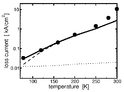 Temperature dependent threshold current density for the mid-infrared type-II 'W' diode lase structure. Dots: Experimental data. Solid line: Total theoretical loss current. Dashed line: Calculated Auger loss current. Dotted line: Calculated radiative loss current. For more details on this example and calculations for radiative and Auger losses see Ref. [40]. Loss in an InGaAsP/InP-structure for 1.3µm 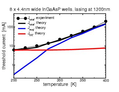 Experimentally measured (black signs) and calculated (thick lines) temperature dependent loss currents at threshold for a structure containing eight 4.4nm wide In0.83Ga0.17As0.67P0.33/InP quantum wells lasing near 1.3µm. The experimental data was extracted from A.F. Phillips, et al., IEEE J. Sel. Topics Quantum Electron., vol. 5, 401 (1999). Black: total loss current; Red: radiative loss current due to spontaneous emission; Blue: Auger loss current. For more details on this example and calculations for radiative and Auger losses see Ref. [28]. Loss in an InGaAs/InP-structure for 1.5µm 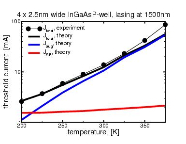 Experimentally measured (black signs) and calculated (thick lines) temperature dependent loss currents at threshold for a structure containing four 2.5nm wide In0.65Ga0.35As/InP quantum wells lasing near 1.5µm. The experimental data was extracted from A.F. Phillips, et al., IEEE J. Sel. Topics Quantum Electron., vol. 5, 401 (1999). Black: total loss current; Red: radiative loss current due to spontaneous emission; Blue: Auger loss current. For more details on this example and calculations for radiative and Auger losses see Ref. [28]. Loss in a GaInNAs/GaAs-structure for 1.3µm 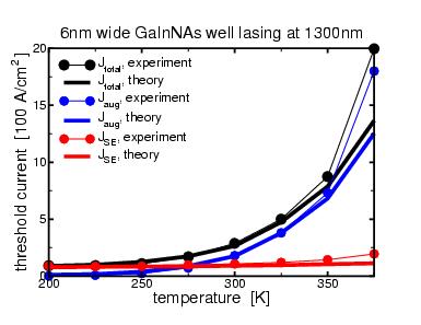 Experimentally measured (thin lines and signs) and calculated (thick lines) temperature dependent loss currents at threshold for a structure with a 6.4nm wide Ga0.66In0.34N0.018As0.982/GaAs quantum well lasing near 1.3µm. The experimental data was extracted from R. Fehse, et al., IEEE J. Sel. Topics Quantum Electron., vol. 8, 801 (2002). Black: total loss current; Red: radiative loss current due to spontaneous emission; Blue: Auger loss current. Losses due to defect recombination have been excluded from the shown experimental data. The deviations between theory and experiment at high temperatures are probably due to internal heating beyond the heat sink temperature. For more details on this example and calculations for radiative and Auger losses see Ref. [28]. Gain in InGaN/GaN 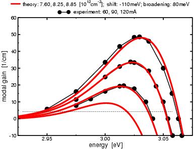 Experimentally measured (black signs) and calculated (red lines) gain spectra for a structure containing of 2nm wide In0.1Ga0.9N quantum wells between 6nm wide GaN barriers. The experimental data was extracted from B. Witzigmann, et al., Appl. Phys. Lett., 88, 021104 (2006). For more details on this example and calculations for wide bandgap nitride systems see Ref. [31] and Ref.[32]. Gain in GaInNAs/GaAs 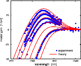 Experimentally measured (blue signs) and calculated (red lines) modal gain spectra for a structure consisting of three 6nm wide In0.32Ga0.68N0.01As0.99 quantum wells between In0.05Ga0.95N0.015As0.985 barriers. The experimental data were obtained with the Hakki-Paoli method. The sheet carrier densities in the calculations ranged from 3.75 to 8.25x10¹²/cm² with increments of 0.75x10¹²/cm², the injection currents in the experiment were 7, 12, 14, 16 and 18mA. For more details see Ref. [1]. 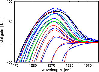 Gain spectra for the same structure as above but for a wider density range. It demonstrates the heating of the device under high excitation conditions, leading to an otherwise unusual red shift of the spectra. The comparison can be used to determine internal temperatures and heating. The experimental data was obtained with a different method than in the example above, which allows to examine a wider density range, but is less accurate. Blue: experimental results for 0, 5, 10, 15, 20, 30, 40, 50, 60 and 70mA. Red: theoretical results for the assumed temperature of 300K and densities of 0, 1.5, 2.5, 3.0, 3.5 and 6.0x10¹²/cm². Green: theoretical results for 312K and 4.5 and 5.0x10¹²/cm². Magenta: 325K, 7.0*10¹²/cm². Black: 337K and 9.0x10¹²/cm². For
more details see
Ref.
[14]. For
more details see
Ref.
[2]. 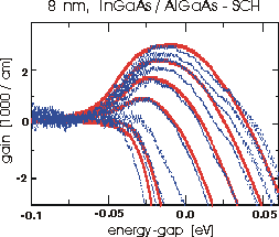 Theory-experiment comparison for a structure consisting of a 8nm wide In0.05Ga0.95As quantum well between Al0.2Ga0.8 barriers. Blue signs show the experimental results, red lines the theoretical ones. The carrier densities in the theory ranged from 0.6 to 3.0x10¹²/cm². The experimental currents are from 0 to 20mA. For more details see Ref. [3]. Absorption in GaInAs/InP-Superlattice 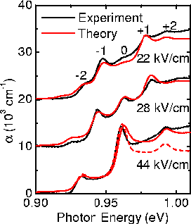 Theory-experiment comparison for the excitonic absorption in a system of electronically coupled InGaAs quantum wells that are separated by thin InP barriers ('superlattice') under different external electric fields. For the case of a field of 44 kV/cm the red dashed line shows the theoretical result if the conduction band nonparabolicity is neglected. The red solid lines have been calculated with this nonparabolicity. The lines for different fields have been shifted along the absorption axis for better clearity. For more details see Ref. [5]. |