Theoretical Models
How Not To Do It
The following are examples showing the severe shortcomings of some approximations
that are still frequently used for the calculation of
• Gain/Absorption,
• Spontaneous Emission,
• Auger recombinations.
For more examples see the SimuLase manual
and our various publications.

Gain/Absorption
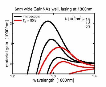
Black lines: Results of the fully microscopic model for the GaInNAs-structure
shown in the examples.
Red lines: Results for the same densities as in the
full model, but with a model that does not calculate the scattering
microscopically but uses a dephasing time to simulate the line
broadening. Otherwise, this model includes all effects (bandgap
renormalization, Coulomb enhancement, band nonparabolicities,...)
the full model does.
The above example demonstrates the errors arisong from using a dephasing
time or a line-broadening instead of calculating
the underlying electron-electron and electron-phonn scattering processes
explicitly. Even if experimental data is known and a decent fit to it can be found for
one carrier density, the fit will fail for higher and lower densities.
Also, spectral positions and the gain amplitude to carrier density relation
will be significantly wrong. This approach requires the previous knowledge
of the experimental result for any decent agreement. Thus, it has no predictive
capabilities but relies on fitting.
These strong general shortcomings are inherent to all attempts using broadenings, no matter
how 'sophisticated' they are. Although some
methods (like 'non-Markovian gain models') avoid e.g. the non-physical absorption
tail energetically below the gain that simple Lorentzian lineshape broadening produces,
however this is merely cosmetics. The underlying microscopic scatterings are strongly dependent
not only on the carrier density but also the temperature and spectral position.
They introduce mixings of the complex microscopic polarisations that lead to
spectral lineshape modifications, amplitude modifications and energy renormalisations
that cannot be captured through broadenings of individual transitions.
The error in the density-amplitude relation would make any attempts to calculate
input-output currents as demonstrated in Close Loop Design
impossible. Since the loss currents scale more than linearly with the carrier density,
errors in the threshold density of several tens of percents would lead to even bigger
errors in the loss currents.
For shortcomings due to neglect of the conduction band nonparabolicity
or the Coulomb induced intersubband coupling see e.g. Ref.[10].

Spontaneous Emission (Photo Luminescence)
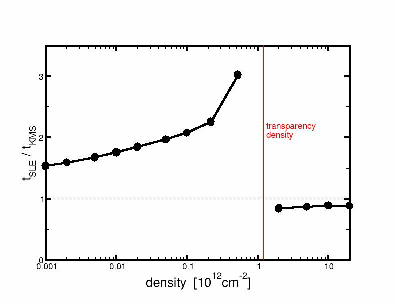
Ratio between radiative carrier lifetimes as calculated with the semiconductor luminescence
equations and those obtained when using the KMS-relation. Here, for the structre investigated in the example for the
Closed Loop Design.
The above picture demonstrates the shortcomings of the Kubo-Martin-Schwinger
(KMS) relation which calculates the spontaneous emission by a simple
integral conversion of the gain/absorption spectra. The KMS relation
is strictly valid only in the absence of any broadenings. However, the correct calculation
of the absorption/gain requires the inclusion of the homogeneous bradening due to
electron-electron and electron-phonon scattering. The KMS-forlmula has a pole at the position
of the chemical potential. If this is energetically in the low energy tail of the
absorption it artificially enhances the spontaneous emission and, thus, leads
to an underestimation of the radiative carrier lifetime which is given by the inverse
of the integral over the spontaneous emission. Thus, the KMS-results can be off by a factor
of two or more.
This error becomes most dramatic
when the chemical potential is just below the bandgap, i.e. for densities just
below transparency. For higher densities the chemical potential is at the position
of the transparency point where absorption/gain is zero. This prevents an artificial pole
in the results. However, as shown in the example above, since the KMS neglects the
excitonic correlations that are included in the luminescence equations, the results
of the KMS are wrong there too and so are in general the lineshapes calculated with KMS.
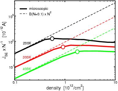
Loss currents due to radiative recombination, JSE, divided by the carrier density.
Bold lines: as calculated with the semiconductor luminescence
equations. Thin lines: using the power law, JSE=BN².
Here, the coefficient, B, was derived by fitting the power law to the low density result of the
microscopic calculation at N=10¹¹/cm². The open signs mark the threshold
carrier densities. Here for the GaInNAs/GaAs-structure investigated
in the examples.
An often used, even simpler approach to calculating the carrier lifetimes due to spontaneous emission than
using KMS is to use a power law, JSE=BN², to describe them.
This power law holds approximately in the limit of very low carrier densities where the carrier distributions
can be described by Boltzmann distributions. However, it fails for densities
where phase space filling becomes significant, i.e. near transparency and above.
Even if as in the example above the exact value for B is known from the low density result,
the results of the power law are off by about a factor of two near threshold and
the error can easily reach one order of magnitude.
It can be shown analytically that for very high densities the density dependence of the radiative losses
changes from quadratically to only linear. This can be seen in the picture above where JSE/N
as calculated microscopically approaches a constant value for high densities.
For more details see e.g. Refs.[28] and
[29].
Auger Recombination Processes
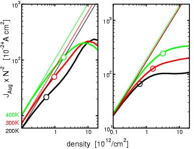
Loss currents due to Auger recombination processes, Jaug, divided by the square of the carrier density.
Bold lines: calculated microscopically.
Thin lines: using the power law, Jaug=CN³.
Here, the coefficient, C, was derived by fitting the power law to the low density result of the
microscopic calculation at N=10¹¹cm². The open signs mark the threshold
carrier densities. Left: for the GaInNAs/GaAs-structure investigated
in the examples. Right:
for the InGaAsP/InP-structure operating at 1.5µm.
Auger recombination losses are often described using a simple power law for the loss current,
Jaug=CN³. Using some rough approximations,
this density dependence can be shown analytically to be correct for low densities where
the carrier distributions can be described by Maxwell-Boltzmann distributions.
However, for in the regime important for laser operation, i.e. near transparency
and above, the density dependence becomes less than cubic. as shown for two
examples in the picture above, here, the density dependence can become only
quadratically (which would yield horizontal lines in the way the data is plotted
in the picture) or even less. Even if as here the correct low density value for
C is known from the microscopic calculation, the results of the power law are
off by a factor of two ore more near threshold. At higher densities, the power
law can lead to an error of one order of magnitude or more.
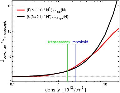
Ratios between microscopically calculated loss currents and loss currents
when using power laws with the coefficients B and C fitted to the microscopic results at low densities.
Red: loss currents due to spontaneous emission. Black: loss currents dur to Auger processes.
Results for the InGaAsP/InP-structure operating at 1.5µm.
The above picture demonstrates as the two previous pictures the shortcomings of the power laws,
JSE=BN² and Jaug=CN³. Near threshold the power laws are off by
a factor of three. For higher densities the error can easily reach one order of magnitude or more.
For more details see e.g. Refs.[28] and
[29].