Theoretical Models
How We do It
All Gain Table calculations are based on state of the art fully microscopic
many-body models. The only input these models require are the nominal structural
design (layer width, material compositions and possible doping concentrations)
and well known basic material parameters that can be found in the standard literature,
like bulk bandstructure parameters (Luttinger parameters, strain constants
and bandgaps), lattice constants, phonon coupling constants, background
refractive indices, dielectric constants and band-offsets.
They do not require or allow any phenomenological fit parameters like line broadenings,
dephasing times or radiative- or Auger-recombination constants. They have been
tested for various materials and device configuration to yield quantitatively
correct results within the scattering of the experiment (see the examples).
Thus, they are truly predictive.
For all calculations we use fully coupled 8x8 kp-bandstructure models
(see Refs.[10], [31]).
For dillute Nitrides
this is coupled to an anti-crossing model for the conduction bands
(see Ref.[8]).
If internal electric fields due to piezoelectric effects or ionized dopants or
external electric fields due to applied Voltages are present, the screening
of these fields by charge inhomogenities is included by coupling the bandstructure
calculation self consistetly to a Poisson solver.
Although not required by the models, Gain Tables generally assume that the carriers
are in thermal equilibrium and can be described by Fermi distribution.
Non-equilibrium effects like carrier relaxation and spectral hole burning and
their influence on spectral properties
can be investigated in a consulting type enviroment.
Details about the theoretical models can be found in the
SimuLase manual and our various
publications.
The typical use of SimuLase™ and data created by it is described for the
examples of an edge emitting device and a VECSEL in the
examples gude.

Gain/Absorption and Carrier Induced Refractive Index
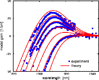
The gain/absorption and carrier induced refractive index changes
are calculated solving the semiconductor-Bloch equations, i.e. the equations
of motion for the microscopic optical polarisations. Here, incoherent
processes, electron-electron and electron-phonon scattering, are
treated explicitely by solving the corresponding quantum-Boltzmann type
scattering equations in second Born-Markov approximation. As demonstrated
here, this is not only
necessary for correct lineshapes, but also for amplitudes and spectral positions.
In these calculations we also include the Coulomb induced inter subband coupling
and the conduction band nonparabolicity.
For more details about this approach see e.g. Ref.[10]
or H. Haug, and S.W. Koch, "Quantum Theory of the Optical and Electronic
Properties of Semiconductors", Fourth Edition (World Scientific, New York, 2004).

Spontaneous Emission (Photo Luminescence) and Radiative Carrier Losses
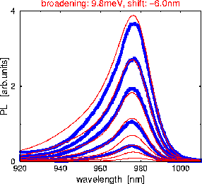
The spontaneous emission and the corresponding radiative carrier lifetime
are calculated using the semiconductor luminescence equations.
These are the microscopic equations of motion for the photon assisted
polarisations and distribution functions. As for the gain calculations,
they involve the solution of quantum-Boltzmann type scattering equations
for electron-electron and electron-phonon collisions. They also
involve the numerically expensive determination of excitonic correlations.
The shortcomings of the often used, numerically much simpler Kubo-Martin-Schwinger
method (a simple integral conversion of absorption/gain spectra into spontaneous emission spectra)
are demonstrated here.
For more details about this approach see e.g. Ref.[28] or
M. Kira, F. Jahnke, W. Hoyer, S.W. Koch, Prog. Quantum Electron. 23, 189 (1999).
Auger Recombination Processes
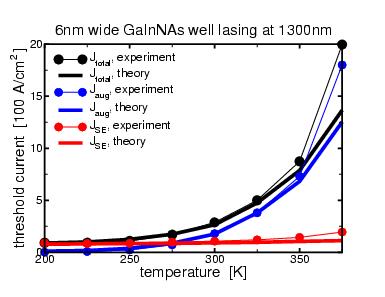
The calculation of carrier recombinations due to Auger processes and
the inverse process, carrier generation due to impact ionisation, requires
to solve complex quantum-Boltzmann type scattering processes in second Born-Markov
approximation. The general equations that have to be solved have been
known for decades. However, mostly due to numerical limitations, previous attempts
to solve them have applied uncontrolled approximations for the involved (Coulomb)
coupling matrix elements, spin-, k-, or band-summations. With these approximations
the accuracy of the results is greatly reduced by up to one order of magnitude or more.
The main difference between our calculations and what has been done in the past
is that we do not use any such approximations but explicitely solve all involved
integrations and summations. As a result, our calculations have been shown
to agree with the experiment within less than a few ten percent uncertainty.
The shortcomings of the use of an Auger constant, C, and a power law, CN³,
instead of calculating the underlying processes explicitly
are demonstrated here.
For more details about this approach see Ref.[28].
For examples of the results of our approach see e.g. the description of the
closed loop design or the examples.